
[ad_1]
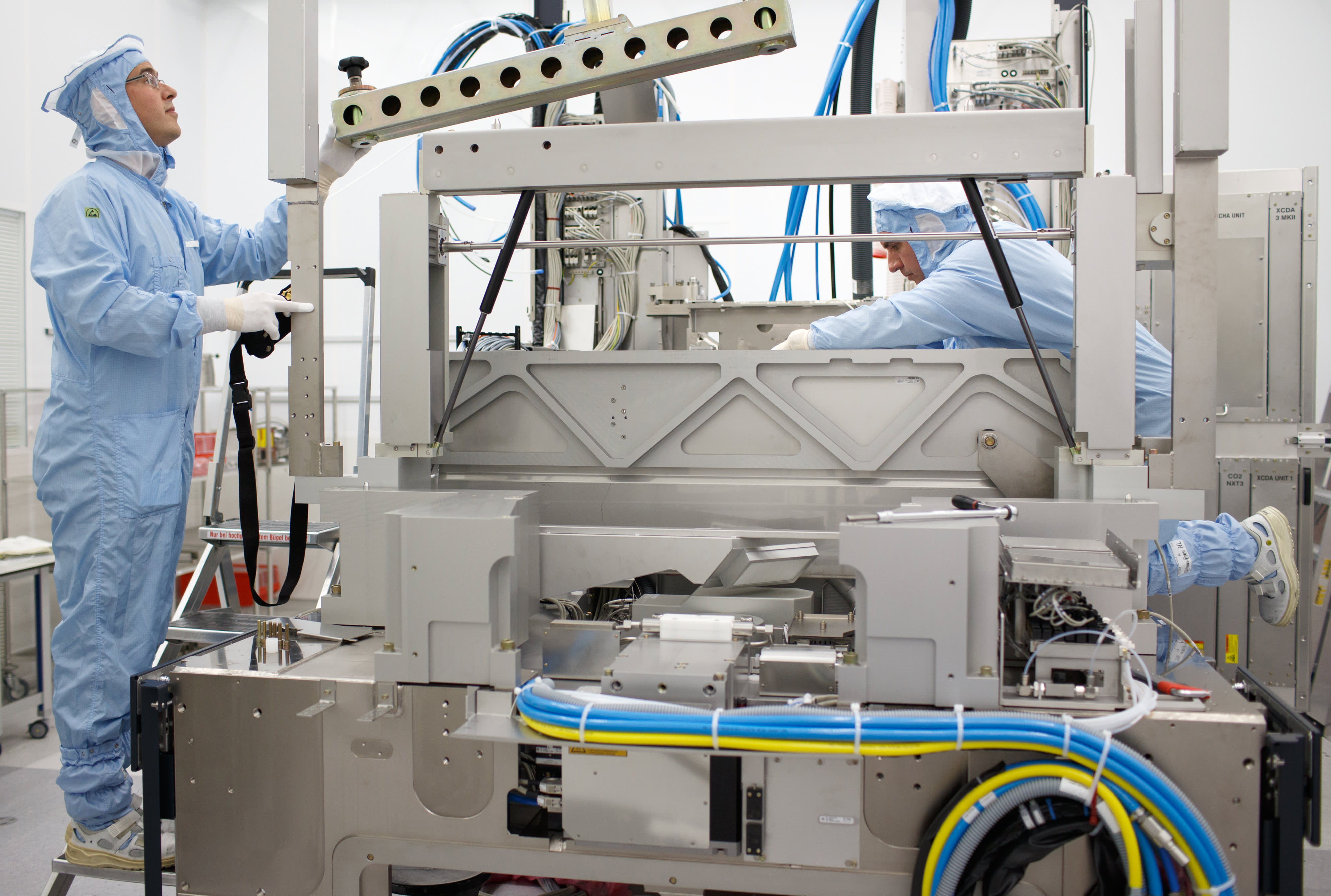
Staff assemble a ASML NXT1970Ci photolithography machine on the ASML Holding NV manufacturing unit in Veldhoven, Netherlands.
Jasper Juinen | Bloomberg | Getty Pictures
With a market worth of round $350 billion, Dutch-headquartered ASML is a little-known tech juggernaut that is set to maintain on rising in step with the insatiable demand for semiconductors.
The 37-year-old firm, which has over 28,000 workers, is the one agency on the planet able to making the highly-complex machines which can be wanted to fabricate essentially the most superior chips.
These machines, which value roughly $140 million every, shine exceptionally slim beams of sunshine onto silicon wafers which were handled with “photoresist” chemical compounds. Intricate patterns are created on the wafer the place the sunshine comes into contact with the chemical compounds, that are rigorously laid out beforehand.
This course of, which ends up in the formation of the all-important transistors, is called lithography. The machines themselves are referred to as excessive ultraviolet lithography machines, or EUV machines.
ASML sells the comparatively uncommon EUV machines to a handful chipmaking giants together with TSMC, Samsung and Intel. Every machine reportedly has over 100,000 parts and it takes 40 freight containers or 4 jumbo jets to ship. Final 12 months, ASML bought simply 31 of those huge items of kit, in keeping with its financials.
The Trump administration even pressured the Dutch authorities to cease the sale of the machine to Chinese language prospects, Reuters reported final 12 months. Consequently, Chinese language chipmakers have been unable to take advantage of superior chips. The Biden administration has proven no indicators of reversing Trump’s stance.
Chris Miller, an assistant professor on the Fletcher Faculty of Legislation and Diplomacy at Tufts College, advised CNBC that chipmakers need to use the narrowest wavelength of sunshine attainable in lithography in order that they will match extra transistors onto each bit of silicon.
Transistors are one of many fundamental constructing blocks of recent electronics they usually allow an electrical present to circulation round a circuit. Typically talking, the extra transistors you may match onto a chip, the extra highly effective and environment friendly that chip shall be.
“The EUV gentle that ASML’s most superior instruments use has a wavelength of 13.5 nanometers, which helps you to carve terribly small shapes on silicon,” stated Miller, who’s within the means of writing a e-book in regards to the historical past of the semiconductor business.
The TSMC chips within the newest Apple iPhones, which have been created with ASML’s EUV machines, have round 10 billion transistors on them, Miller added.
Past lithography, there are a number of different manufacturing processes that have to be accomplished earlier than a chip is prepared for transport. “Finally what you are attempting to do is construct buildings on the silicon utilizing a mixture of carving issues out and depositing new chemical compounds onto it,” Miller stated.
Mirrors and lasers
Given nobody else could make EUV machines which can be appropriate for mass manufacturing, ASML has a monopoly on the section and there is no signal of anybody catching up.
“ASML is completely crucial to the whole semiconductor ecosystem,” Peter Hanbury, a semiconductor analyst at Bain & Co, advised CNBC. “In some methods it is simply as necessary as TSMC.”
He added: “Each bleeding edge chip, beginning at 5 nanometers, and going ahead for possible a really very long time, goes to be closely reliant on ASML tools.”
Semiconductor analysts imagine it could take round a decade and billions of {dollars} for one more firm to get to a stage the place it may begin to compete with ASML.
“ASML has round 4,000 suppliers that they are conscious of and their suppliers have suppliers as effectively,” stated Miller.
A few of the key parts in ASML’s EUV machines are notably troublesome to make.
The mirrors, for instance, are made by German agency Zeiss in partnership with ASML they usually’re the flattest buildings people have ever made.
“These buildings themselves are type of marvels of engineering,” Miller stated. In comparison with regular mirrors, they’re comparatively reflective, which is necessary as a result of chipmakers don’t desire photons to be misplaced earlier than the beams of sunshine come into contact with their wafers.
The toughest a part of the EUV machine to make, nonetheless, is the sunshine supply, which has come a great distance through the years. “Traditionally, they [chipmakers] simply used a light-weight bulb within the 60s and 70s,” Miller stated. “Gentle bulbs do not emit excessive ultraviolet gentle and it is arduous to get sufficient energy [or] sufficient photons emitted.”
The sunshine supply in ASML’s EUV machine emits tiny balls of tin, about 30 microns broad, which can be blasted twice by the world’s strongest carbon dioxide lasers. The primary blast “will get it prepared” and the second, stronger pulse turns it right into a plasma which is 400,000 levels Fahrenheit in temperature, Miller stated.
“This plasma of exploded tin, if you’ll, emits photons of maximum ultraviolet gentle,” Miller stated. “Making this course of work took 30 years.”
ASML’s EUV machines are primarily made at a facility within the Netherlands, however there’s additionally a web site in Connecticut the place some tools is made.
“It is an insane course of to ship them,” stated Miller. “Then there is a large studying course of to get them up and operating as a result of the machines are so sophisticated. They are not like an off the shelf, plug it in, flip it on and go. You want to have the ability to practice the workers which can be working them.”
ASML workers are primarily based contained in the chip foundries the place the machines get deployed, Miller stated, including that they monitor and tweak the EUV machines at any time when crucial. “There’s solely a pair dozen of those machines in operation worldwide. They’re nonetheless studying how they really work.”
Upcoming gross sales growth?
Demand for ASML’s EUV machines is hovering as chipmakers try to beat a world crunch.
In September, ASML stated it expects a gross sales growth over the following decade. It believes annual income will hit 24-30 billion euros by 2025, with gross margins as much as between 54% and 56%. The prediction is considerably larger than the 15-24 billion euro vary it had beforehand forecast.
“We see important development alternatives past 2025,” the corporate stated, including that it expects to attain an annual income development fee of round 11% between 2020 and 2030.
ASML stated “world megatrends within the digital business” coupled with “a extremely worthwhile and fiercely modern ecosystem” are anticipated to proceed to gas development throughout the semiconductor market, which is battling the worldwide chip scarcity.
It added that development in semiconductor markets and “growing lithography depth” are driving demand for its services.
Over the past 12 months, ASML’s share value on Amsterdam’s inventory change has gone from round 350 euros to 772 euros on Nov. 19. Shares have been buying and selling at an all time excessive on Friday final week.
In October, two tech buyers, Ian Hogarth and Nathan Benaich, predicted that ASML will turn out to be a $500 billion firm by the tip of 2022.
“As individuals search for alpha when investing on this pattern of semiconductors being increasingly crucial to world provide chains, this [ASML] feels prefer it’s an apparent candidate,” angel investor Ian Hogarth advised CNBC.
Miller stated there’s loads of causes to anticipate ASML’s gross sales to develop.
“We’re simply within the early phases proper now with EUV,” he stated, including that EUV machines have solely been utilized in high-volume manufacturing for a few years.
In that point they have been used to assist create a whole lot of tens of millions of chips, however most of ASML’s key prospects are actually simply starting to roll out EUV in a critical approach, in keeping with Miller.
ASML is not resting on its laurels both. The corporate is planning to launch a subsequent era machine referred to as Excessive-NA, which stands for top numerical aperture, round 2025.
“It can enable much more particular etchings on silicon chips,” Miller stated, including that Intel has signed an unique (and doubtless very costly) deal to get the primary Excessive-NA machines.
“Except you assume that our demand for computing energy goes to stagnate or decline, which does not appear to be a secure guess from my perspective, I believe the expectation’s obtained to be that ASML’s income retains rising,” Miller stated.
[ad_2]
Source link


